This is Part 4 of the Memory in the AI Era series. Part 1, Part 2, and Part 3 covered High Bandwidth Flash (HBF), which fills an empty seat in the memory hierarchy right next to the GPU. From this part on, we shift our viewpoint outside the GPU, to the system level, and look at where Compute Express Link (CXL) fits in the memory hierarchy.
Introduction
Hello, I’m Seungbin Shin, an RTL Designer at HyperAccel.
Across Parts 1-3, we took a deep look at the memory layer right next to the GPU. HBM stacked DRAM to push up bandwidth, and HBF wrapped NAND in HBM’s packaging to bring in capacity.
But when you talk about data center memory, there’s a name that keeps coming up from a seat other than the one next to the GPU. That name is CXL.
It’s the keyword that never fails to appear in conversations like “building a memory pool,” “sharing memory between VMs,” or “tiering an AI server’s hot/warm/cold data.”
And yet, when you actually search for CXL, even the acronyms are bewildering. There’s CXL.io, CXL.cache, and CXL.mem; there are Type 1/2/3 devices; and the versions run from 1.1 to 2.0, 3.0, 3.1, and 3.2. It’s an interface with a fairly high barrier to entry.
So in this part, I want to start from a single question.
“We already have both DDR and PCIe — so why was yet another new interface needed?”
Answering this question naturally reveals where CXL settles in the memory hierarchy, and why the big three memory vendors (Samsung, SK hynix, Micron) are all scaling up their CXL product lineups at once.
The content of this post is based on my personal study and experience. If you find any errors, please let me know in the comments.
Why Yet Another Interface — The Empty Seat Between DDR and PCIe
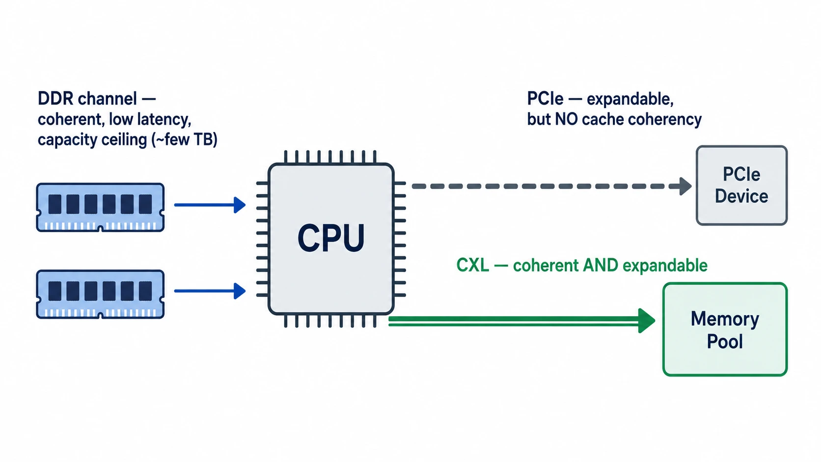
The short answer: DDR can’t be scaled up, and PCIe is hard to use as memory.
Within a single server, there are broadly two paths the CPU uses to move data.
- DDR channels: a memory-dedicated bus connecting to the DRAM modules right next to the CPU
- PCIe: a general-purpose serial bus connecting to peripherals like GPUs, NICs, and SSDs
Each path has a clear role it does well. But both paths have hit their limits.
The Limit of DDR: The Channel Count Is the Ceiling
To attach more DDR DRAM, the CPU has to add more memory channels. But adding channels increases the pin count on the CPU package, and the motherboard wiring grows more complex along with it.
Even the latest generations of server CPUs top out at around 8-16 channels, with the number of modules per channel limited to 1-2.
As a result, the DRAM capacity of a single socket is capped at a few TB. Beyond that, it’s physically impossible to attach more.
As the data an LLM inference node handles (KV cache, model weights, embeddings) swells to tens of TB, brushing up against this ceiling is becoming more and more common.
The Limit of PCIe: Fast, But No Coherency
So what if we attach memory over PCIe? On a 16-lane link, PCIe Gen5 provides about 64 GB/s per direction (128 GB/s aggregate across both directions). That’s comparable to a single DDR5 channel (about 50 GB/s).
As it happens, this 64 GB/s figure already showed up in Part 3 — it’s the very same PCIe that was singled out as the “bandwidth ceiling” when attaching HBF next to the GPU. But from the standpoint of memory expansion, the bandwidth itself isn’t really lacking. The real obstacle lies elsewhere.
There are two problems when you attach memory over PCIe.
First, there’s no cache coherency. Cache coherency is the property that, even when multiple agents (CPU cores, devices) each cache the same memory address, a change by one is always reflected so the others see the latest value. DDR memory sits inside the CPU’s coherency domain, so the CPU’s cache hierarchy and memory controller maintain this automatically; PCIe sits outside that domain. For the CPU to directly load/store the memory of a PCIe device, this coherency has to be guaranteed at cache-line granularity. PCIe is fundamentally a packet-based I/O protocol, so it offers no such guarantee. To use PCIe memory like main memory, the OS has to explicitly copy the data over (e.g., via memcpy).
Second, the memory semantics are coarse. PCIe operates in transaction units larger than the 64B cache line. You can’t do fine-grained access in the small units that memory requires.
You can attach memory over PCIe, but from the CPU’s point of view, that memory is “someone else’s memory,” not “my memory.”
The Empty Seat: A Cache-Coherent Memory Interface
If we tie everything so far into a single line, it’s this:
We need something that is a coherent memory interface like DDR, yet can extend outside the system like PCIe.

The standard that emerged to fill this empty seat is exactly CXL.
CXL is not a physical layer built from scratch. It’s a standard that borrows PCIe’s physical layer (PHY) as-is and layers a new, cache-coherent protocol on top of it.
A high-speed interconnect standard that adds a cache-coherency contract on top of the off-the-shelf PCIe 5.0 infrastructure — that’s the core idea of CXL.
The Three Faces of CXL — CXL.io / CXL.cache / CXL.mem
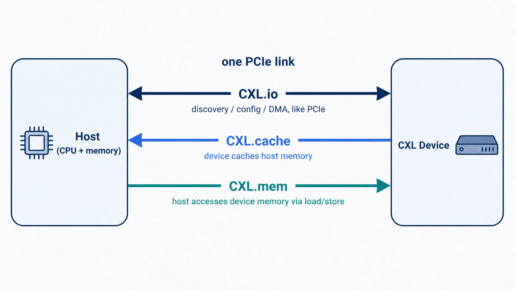
CXL isn’t a single protocol but a bundle of three sub-protocols. All three flow simultaneously over a single PCIe link.
| Sub-protocol | Role | Model |
|---|---|---|
| CXL.io | Device discovery, configuration, DMA | Same as PCIe |
| CXL.cache | Device caches host memory | Device → Host |
| CXL.mem | Host directly accesses device memory | Host → Device |
The names alone are confusing, so let me unpack each role.
CXL.io — The Same Foundation as PCIe
CXL.io is effectively identical to PCIe. It handles discovering devices (enumeration), reading configuration space (configuration), delivering interrupts, and moving large data via DMA.
Every CXL device must implement CXL.io. This is exactly why CXL was built as a standard layered on top of PCIe — so that the existing PCIe infrastructure (OS drivers, BIOS, controller IP) can be reused as-is.
CXL.cache — The Device Caches CPU Memory
Consider a case where a device like a GPU or an accelerator frequently reads the CPU’s main memory.
With PCIe, you’d have to fetch the data from main memory every time. But what if you put a small cache inside the device and stored frequently used data there? As long as there’s a guarantee that the CPU and the device are looking at the same data, you could dramatically cut down on communication.
CXL.cache does exactly this. It lets a device cache host memory at cache-line (64B) granularity and keeps that cache coherent with the CPU’s caches.
Internally, it’s a way of extending the CPU’s cache-coherency protocol (e.g., MESI) across the CXL link. What state (Modified/Exclusive/Shared/Invalid) a device takes a cache line in, and how to handle the case where another caching agent already holds that line — all of it is standardized.
CXL.mem — The CPU Treats Device Memory Like Main Memory
There’s also the reverse direction. This is the case where you attach a lot of memory (DRAM, or beyond) to a device, and the CPU wants to load/store that memory like its own main memory.
CXL.mem takes on this role. From the CPU’s perspective, the device memory appears as a region within its own physical address space, accessible directly with ordinary load/store instructions.
The important point here is that the CPU plays the role of the home agent. In a case like Type 3, where the device only holds memory, it’s enough for the host to manage coherency on its own.
By contrast, in a case like Type 2, where the device also has its own cache, bias-based coherency is applied — explicitly marking whether the “owner” of a given cache line is the device or the host. Since whichever side owns the line is responsible for its coherency, bidirectional coherency traffic can be greatly reduced.
It sounds complex, but the actual implementation burden is fairly light on the device side. For Type 3, the device just has to respond to read/write requests like a memory controller.
Combining the Three Protocols
A CXL device picks and implements among the three protocols depending on what it does.
- A device with no memory of its own that only caches host memory: CXL.io + CXL.cache
- A device that has memory and just needs the host to use it like its own memory: CXL.io + CXL.mem
- A device that has memory and also needs to cache host memory: CXL.io + CXL.cache + CXL.mem
These three combinations become the basis for the Type 1 / Type 2 / Type 3 devices covered in the next section.
What Do You Plug In — Type 1 / 2 / 3 Devices
Depending on how you combine the three sub-protocols, CXL devices fall into three types.
| Type 1 | Type 2 | Type 3 | |
|---|---|---|---|
| Protocols used | CXL.io + CXL.cache | CXL.io + CXL.cache + CXL.mem | CXL.io + CXL.mem |
| Device’s own memory | None | Yes | Yes |
| Caches host memory | Yes | Yes | No |
| Representative example | SmartNIC, FPGA accelerator | GPU, AI accelerator | Memory expansion module |
Let me unpack the role and use cases of each type.
Type 1 — The Accelerator That Only Caches
A Type 1 device has no memory of its own and caches host memory.
The representative candidate is the SmartNIC. When processing packets coming in from the network, it frequently reads the host’s descriptor queues and packet buffers. Instead of making a round trip all the way to host memory every time, keeping these in the NIC’s internal cache and maintaining coherency can greatly reduce packet-processing latency.
Type 1 shows its value in workloads that frequently reference host data structures, as with FPGA accelerators.
Type 2 — The Accelerator With Both Memory and Cache
A Type 2 device has its own memory and also caches host memory. It uses all three protocols.
The typical example is a GPU or AI accelerator attached over CXL. The accelerator has its own HBM/GDDR, but it also fetches and caches model weights or input data from host memory. It pulls host data via CXL.cache and exposes the accelerator’s memory to the host via CXL.mem.
The catch is that Type 2 is the most complex type to implement. Since coherency has to be managed in both directions, the burden on the device-side controller is large. That’s why there aren’t many Type 2 devices in actual mass production yet.
Type 3 — The Most Commonly Seen Memory Expansion Module
A Type 3 device only has its own memory and does not cache host memory. It only needs to implement CXL.io and CXL.mem.
Put simply, it’s “a memory module with a CXL interface.” From the host’s perspective, it looks like a DDR module placed one step farther away, accessible with ordinary load/store.
Most of the CXL products currently in mass production — or right on the verge of commercialization — are Type 3. The reasons are clear.
- It has the lowest implementation complexity,
- it most directly relieves the DDR channel ceiling, and
- it leads naturally into the product lineups of existing memory vendors.
The CXL Memory Module (CMM) lineups from the big three memory vendors, which we’ll look at later, are all Type 3 as well.
From a Single Device to a Fabric — CXL 1.1 → 2.0 → 3.x
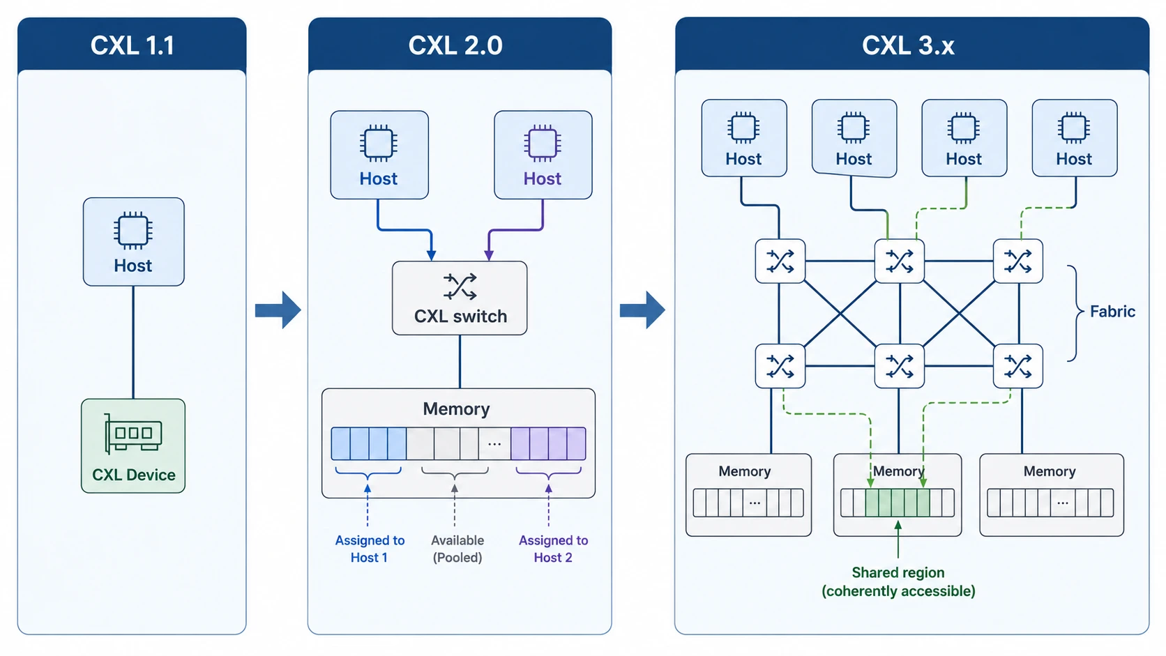
CXL has been evolving rapidly since 1.0 came out in 2019. The features added in each version ultimately point in one direction.
Letting memory be placed farther, in greater amounts, and shared by more hosts.
Let me touch on the key change in each version.
CXL 1.1 — Directly Connected to a Single Host
This is the most basic form. A single CXL device is connected directly, like a PCIe slot, to a single host CPU.
At this stage, CXL is a tool for “attaching extra memory one step farther out, next to DDR.” Increasing the memory capacity of a single node is the main goal; it doesn’t extend to other nodes’ memory.
CXL 2.0 — The Switch and Memory Pooling
In 2.0, which arrived in 2020, a decisive change occurs. The CXL switch is introduced, making it possible to weave multiple hosts and multiple memory devices together like a mesh.
The most striking application is memory pooling. Data center memory utilization averages around 40-50%. It’s common for some servers to be short on memory while others sit more than half empty.
In CXL 2.0, multiple hosts can dynamically allocate as much as they need from a single memory pool.
There’s one thing to be careful about. The “sharing” here is dynamic allocation, not concurrent sharing.
A large memory device is split into multiple chunks in the form of a Multi-Logical Device (MLD). A control plane called the Fabric Manager (FM) then hands them out: “this chunk to host A, that chunk to host B.” A single chunk is owned by only one host at any given moment. So there’s simply no region where a cache-coherency conflict could even arise.
To use a hotel-room analogy: a single room (chunk) is rotated as one guest (host) checks in and out — two guests don’t enter the same room at the same time.
This model alone is enough to reduce the practice of over-buying memory for each server based on worst-case assumptions. At this stage, CXL is no longer a single-node expansion interface. It begins to become the foundation for rack-level memory resource management.
CXL 3.x — The Fabric and Multi-Host Coherence
The flow continuing through 3.0 (2022), 3.1 (2023), and 3.2 (2024) gets even more ambitious.
There are two key points.
First, from dynamic allocation to true sharing. Where 2.0’s pooling was “one chunk = one host at a time (rotated between hosts),” in 3.x multiple hosts read and write the same memory region simultaneously while hardware maintains cache coherency. This is also called Global Fabric Attached Memory (GFAM). Allocation (granting access) doesn’t disappear here either — the difference is that where 2.0 gave one chunk to one host exclusively, 3.x lets the Fabric Manager grant multiple hosts simultaneous access to the same region. From this stage on, real conflicts can occur, and the home agents on the host and device resolve them at cache-line granularity.
Second, from port-level connections to a fabric connection. 3.x ties together many CXL switches to form a large-scale fabric. Here, Port-Based Routing (PBR) routes by destination port ID — which, unlike the older tree structure, lets devices be arranged in various topologies such as mesh, dragonfly, and 3D torus, and scales to large device counts.
Once you reach this stage, CXL effectively establishes itself as a new interconnect standard inside the data center. It even starts to become a point of comparison with accelerator interconnects like NVIDIA’s NVLink and UALink (an open standard for connecting accelerators).
As of 2026, most products in mass production support CXL 2.0. The 3.x standard is out, but support in actual devices and host CPUs is only just catching up.
The CXL Blueprint the Big Three Memory Vendors Are Drawing
Now that we’ve covered the big picture of CXL, let’s come down to actual products.
What’s interesting is that even though the standard is led by consortium members like Intel, AMD, Microsoft, and Meta, the side rolling out mass-production product lineups most aggressively is the big three memory vendors. Samsung, SK hynix, and Micron each announced CXL memory modules of a similar shape at nearly the same time.
Here’s a summary of the three companies’ product lineups.
| Company | Representative product | Form factor | Key feature |
|---|---|---|---|
| Samsung | CMM-D (CXL Memory Module - DRAM) | E3.S | Simple memory expansion, CXL 2.0 |
| Samsung | CMM-B (CXL Memory Module - Box) | Box appliance | Rack-level memory pooling |
| Samsung | CMM-H (CXL Memory Module - Hybrid) | E3.S | DRAM + NAND hybrid |
| SK hynix | CMM-DDR5 | E3.S | DDR5-based memory expansion |
| SK hynix | CMM-Ax | E3.S | Memory + compute engine integration |
| Micron | CZ120 / CZ122 | E3.S | Memory expansion module |
It stands out that most use the E3.S form factor. It’s a hot-swappable standard form factor commonly seen in server storage, and since there’s already accumulated know-how for data center deployment, the adoption barrier is low.
Capacities run around 96 GB - 256 GB depending on the model, and the interface commonly uses PCIe Gen5 x8. The three companies’ specs are surprisingly similar. The real difference comes down to “will you stop at a memory module, or take it one tier further?”
The First Line: Honest Memory Expansion (Type 3 As-Is)
The most basic product is simply a DDR5 memory module with a CXL interface.
- Samsung’s CMM-D, SK hynix’s CMM-DDR5, and Micron’s CZ120/CZ122 all fall into this category.
- From the host’s perspective, it looks like “a DDR module placed a bit farther away,” accessed with ordinary load/store.
The target workload is clear. It’s workloads that have hit the per-socket DRAM capacity ceiling.
- in-memory DBs and large-scale analytics
- KV cache and embedding stores placed on the CPU side in LLM inference
- memory-starved nodes in VM consolidation environments
This is the first battleground, where the three companies compete with nearly identical specs.
The Second Line: Pooling and Compute Beyond the Module
The truly interesting side is next. The big three memory vendors don’t stop at simple expansion modules; they’re trying to pull CXL’s follow-on features (pooling, compute) into their own products.
There are two representative directions.
Bundling into a pooling box. Samsung’s CMM-B (Box) packs multiple CMM-D cards into a single appliance to form a rack-level memory pool. It embeds a CXL 2.0 switch so that multiple hosts can allocate as much memory as they need from this box.
Putting a compute engine inside the memory module. SK hynix’s CMM-Ax is the representative example, and Samsung draws a similar picture with CMM-H and CXL-PNM.
This idea is one branch of Near-Memory Processing (NMP) or Processing-in-Memory (PIM). Instead of fetching data and then computing, it’s a way of computing right where the data is and bringing back only the result.
The candidate workloads are things like:
- vector embedding similarity comparison (RAG)
- database filtering and aggregation
- some stages of LLM inference (e.g., KV cache compression, top-k selection)
For this model to be meaningful, it has to be a workload where the cost of moving data across CXL is greater than the cost of computing it. Here, “cost” means the time (latency) of moving the data and the bandwidth and power it consumes. Instead of pulling a huge embedding collection over to the host for similarity comparison, finishing it inside the memory module and passing back only the result reduces both traffic and latency.
The HBF + HAVEN combination covered in Part 2 — the idea of placing a huge vector DB on HBF and attaching a search engine right next to it to finish RAG similarity comparison on the spot — reappears in the CXL space as an NMP-integrated module.
The Fabric and IP Camp — From Controllers to Switch Silicon
Beyond the big three memory vendors, there are players who never go missing from the CXL ecosystem. These are the companies that supply CXL controller/switch IP, or build their own silicon directly.
- Astera Labs: Its Leo series controllers are used in Microsoft Azure’s M-series CXL memory and elsewhere, aiming for the position of the “standard part” of CXL memory controllers.
- Marvell, Microchip (formerly Microsemi): They hold one axis of the IP camp with their controller lineups. The Micron CZ120 we saw earlier also uses Microchip’s SMC 2000 controller.
- Panmnesia: A Korean fabless startup that came out of KAIST’s CAMELab (Computer Architecture and Memory Systems Laboratory). There’s an interesting connection here. M. Jung, an author of the Memory Pooling With CXL paper cited in the references, is Professor Myoungsoo Jung of KAIST, who founded this company. It doesn’t stop at controllers — it’s a full-stack player that builds even CXL 3.2 fabric switch silicon (PANSWITCH) directly. It’s implementing 3.x’s most cutting-edge features, such as PBR and mesh/dragonfly/3D torus topologies, in silicon ahead of anyone else. In April 2026 it announced a second-half mass-production plan along with the supply of pre-release silicon, stepping into a full-fledged commercialization phase.
Memory companies do sometimes design their own CXL controllers, but since the standard evolves so quickly, it’s common to outsource to — or collaborate with — IP/silicon suppliers. Especially in an area like the 3.x fabric, where the standard itself is only just settling, specialist players like Panmnesia appear to be a step ahead — a pretty interesting point even from the perspective of the Korean semiconductor ecosystem.
Why the Memory Companies Are All Entering CXL at Once
There’s a common motivation behind the three companies releasing products in the same category at nearly the same time.
It’s an opportunity for memory to move up a level — from “a module you plug in” to “a seat it occupies within the system.”
Concretely, there are three effects.
- Expanding sellable capacity per node: they can sell more memory beyond the DDR channel ceiling
- Room to raise module pricing: differentiation through add-on features like pooling and NMP
- Entry into the solutions business: proposals not just as a simple component, but at the level of a pooling appliance (e.g., CMM-B)
If HBM grew the memory business next to the GPU, CXL is a card that can regrow the memory business next to the CPU — at the system level. That’s why it’s not strange at all that the three companies are releasing similar product lineups at similar times.
So Is It Actually Usable — The Remaining Homework
Hearing all this, CXL might look like a cure-all, but at the actual adoption stage there’s homework you can’t ignore.
Latency Tax
Memory attached over CXL is slower than direct-attached DDR memory.
- DDR5 native: about 80-100 ns
- CXL memory (Type 3): about 170-300 ns
That’s about 2-3x the latency. This is an intrinsic cost that comes from the structure of layering a protocol on top of the PCIe PHY.
Given this cost, CXL memory naturally enters not as a replacement for all of main memory, but as the second tier in a 2-tier memory configuration of “nearby DDR + one-step-farther CXL.”
Software Stack Maturity
From the CPU’s perspective, CXL memory looks like “a slightly slow NUMA node.” So the OS and runtime have to decide which data to keep in nearby DDR and which to send to CXL.
The Linux kernel is rapidly putting the CXL driver, hot/cold page tracking, transparent page migration, and so on in order, but per-workload optimal tuning still needs time.
In particular, for a workload with a deterministic memory access pattern, like LLM inference, it’s more efficient for the application to decide data placement directly than to rely on the OS’s automatic tiering. This is still an area with plenty of room to pioneer.
The Empty Seat of Type 2, the Type 3-Centric Reality
On paper, Type 1/2/3 are all defined, but the actual market runs around Type 3. This is due to the combination of Type 2’s bidirectional-coherency complexity and the fact that GPU vendors are pushing their own interconnects (NVLink and the like).
Whether CXL really goes all the way to being “the accelerator interconnect standard,” or settles in as a memory expansion + pooling standard, is still an open question.
Wrapping Up & Next Installment Preview
In this post, we looked at what empty seat CXL fills in the memory hierarchy and what parts it’s made of.
Here’s the summary:
- The empty seat: DDR has a clear channel ceiling within a single node, and PCIe has no coherency, so it’s hard to use as memory. The seat in between.
- The three faces: CXL.io (same as PCIe), CXL.cache (the device caches the host), CXL.mem (the host directly accesses device memory).
- The three types: Type 1 (cache only), Type 2 (memory + cache), Type 3 (memory expansion). The market is Type 3-centric.
- Standard evolution: 1.1 (single host) → 2.0 (switch, pooling) → 3.x (fabric, multi-host coherence).
- The big three’s CMM: the first line is honest memory expansion (Samsung CMM-D, SK hynix CMM-DDR5, Micron CZ120). The second line is the pooling box (Samsung CMM-B) and compute integration (SK hynix CMM-Ax, Samsung CXL-PNM).
- The remaining homework: a 2-3x latency tax, an immature software stack, and the empty seat of Type 2.
That said, this post has only answered the “what is CXL” stage. The truly interesting question is next:
How is CXL actually used in real LLM serving workloads, and which workloads does it fit well?
In the next Part 5, we’ll look at concrete use cases that leverage CXL — KV cache offload, VM consolidation through memory pooling, and hot/warm/cold tiering — and at where the big three’s CMM lineups can fit within them.
P.S.
I’m designing RTL at HyperAccel for the launch of an LLM acceleration ASIC chip. Extending the memory hierarchy from next to the GPU out to outside the GPU, all the way to the system level, makes the problems an accelerator designer has to solve even more varied. I hope this series helps us understand the flow of memory technology together and watch the changes ahead.
HyperAccel is a company that covers HW, SW, and AI, bringing together outstanding talent across all domains. If you want to learn broadly and deeply while growing together, please apply to HyperAccel anytime!
Careers: https://hyperaccel.career.greetinghr.com/ko/guide
Reference
- Compute Express Link Consortium — Specifications
- CXL 3.1 Specification Overview
- Intel — Compute Express Link Technology
- Samsung — CXL Memory Module (CMM-D / CMM-B / CMM-H)
- SK hynix CMM-DDR5 / CMM-Ax Product Briefs
- Micron CZ120 / CZ122 CXL Memory Expansion Module
- Astera Labs Leo CXL Smart Memory Controllers
- Panmnesia — Full Stack CXL Link Solution
- Panmnesia PANSWITCH — CXL 3.2 / PCIe 6.x Fabric Switch (pre-release silicon Apr 2026, mass production H2 2026)
- Linux Kernel CXL Documentation
- D. Gouk, M. Kwon, H. Bae, S. Lee, M. Jung, “Memory Pooling With CXL,” IEEE Micro, vol. 43, no. 2, pp. 48-57, 2023. DOI: 10.1109/MM.2023.3237491
- D. Das Sharma, R. Blankenship, D. S. Berger, “An Introduction to the Compute Express Link (CXL) Interconnect,” ACM Computing Surveys, vol. 56, no. 11, Article 290, 2024. DOI: 10.1145/3669900 (arXiv:2306.11227)