Know Your Enemy, Know Yourself, Part 2 : TPU Emergence and Rise
Know Your Enemy, Know Yourself, Part 1: GPU History and Fundamentals
Know Your Enemy, Know Yourself
This means that if you know your enemy and know yourself, you will not be imperiled in a hundred battles.
This series aims to deeply understand competitors’ hardware for AI accelerator design.
In this second article, we cover Google’s TPU (Tensor Processing Unit), which has recently declared its entry into the AI accelerator market.
What is TPU?
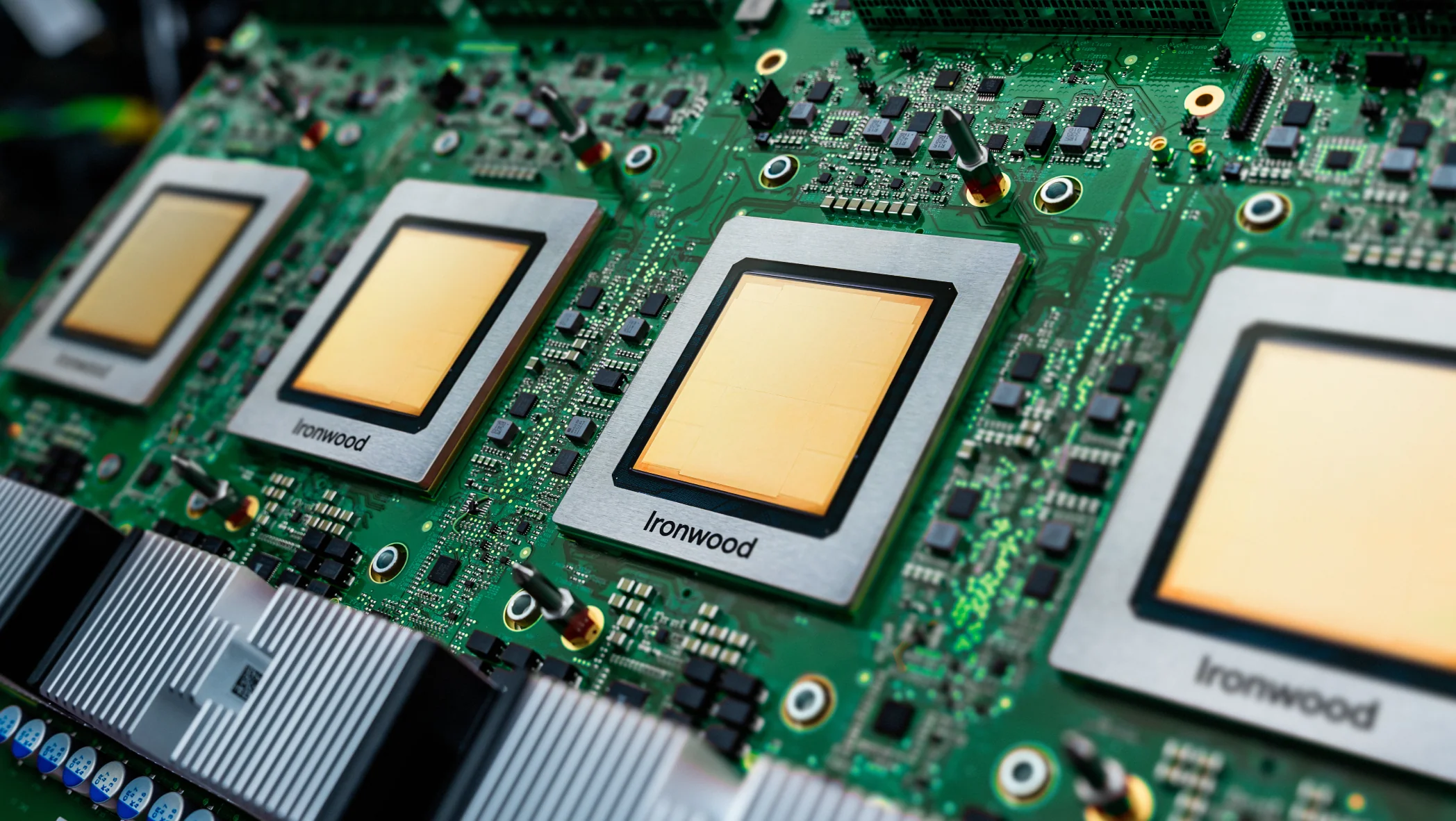
TPU has become one of the hottest keywords in the AI accelerator market. Last November, Google introduced Ironwood, the 7th-generation TPU architecture, announcing improved training and inference performance, cluster scalability, and collaboration with AI startup Anthropic. Both domestic and international media have covered this extensively, making TPU a known term to the general public, and this news has significantly impacted the stock prices of both Google and NVIDIA.
However, TPU is not a product that suddenly appeared. The recently announced TPU is the 7th generation. Google has been releasing new generations of TPU every year since 2016. Initially used only for internal model development and research, including AlphaGo, Google has also sold services through Google Cloud that allow other companies and research institutions to use TPU.
But when you think about it, it’s strange. Google is clearly a software company, so why did they create their own chip instead of using GPUs? And where does the confidence to enter the hardware market come from? Today, we will explore the origins of TPU and the latest generation Ironwood to understand Google’s ‘well-founded confidence’ in the AI semiconductor market.
The Emergence of TPU
To understand the TPU structure, we must first understand the background of TPU development. This is detailed in the TPU 1st generation paper.
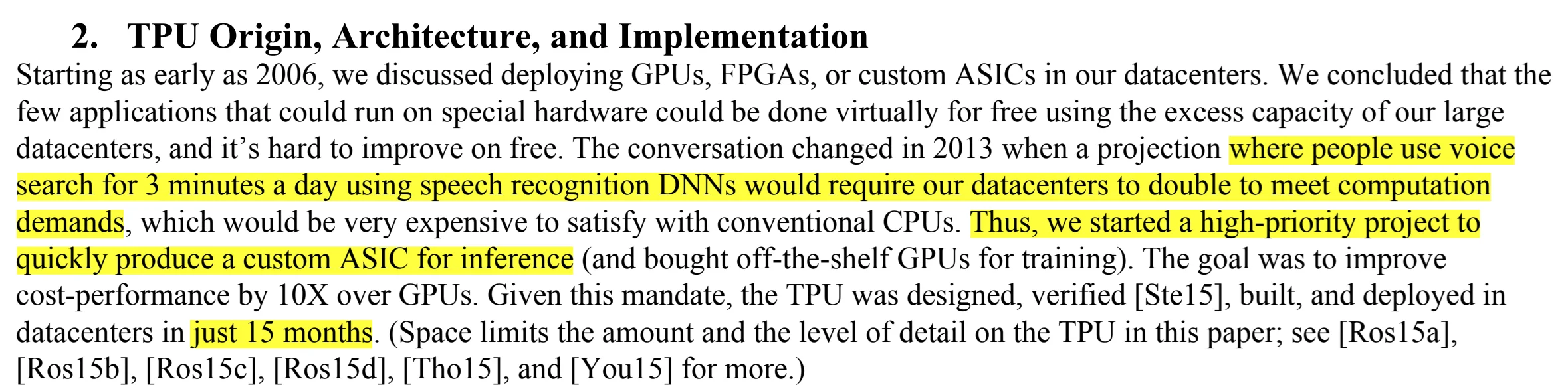
In the 2000s, Google’s services could handle even tasks requiring special types of computation using idle resources in existing data centers without needing custom ASICs. However, as AI technology was fully integrated into Google services in the 2010s, the situation changed. When assuming people use voice search for just 3 minutes per day, predictions showed that running deep neural networks (DNN) for voice recognition would require doubling the scale of existing data centers. As general CPUs could no longer handle this, Google internally started a custom ASIC project, the TPU project. The remarkable thing is that design, verification, manufacturing, and deployment were completed in just 15 months. The TPU produced at that time was used only internally at Google until 2016, when it was revealed that TPU was used in the match between Lee Sedol and AlphaGo, making TPU known to the outside world for the first time.
TPU Hardware Architecture
Now let’s examine the TPU architecture in detail.
Systolic Array
As mentioned earlier, TPU was designed specifically for AI operations. The biggest characteristic of AI operations is performing large-scale matrix multiplication. This is a common feature seen in the process of using artificial neural network weights and computing other values during training and inference, regardless of model type (CNN, RNN, Transformer).
TPU uses a special unit called Systolic array, which cannot be found in general processors (CPUs), to efficiently execute this matrix multiplication. The term “Systolic” is derived from “systole,” the contraction phase of the heart. Just as the heart rhythmically beats and sends blood to various parts of the body, data moves rhythmically and regularly between computational units within the array structure, performing operations - hence the name. Systolic array optimizes data flow and maximizes parallel processing, making it efficient for large-scale operations like matrix multiplication. The process of Systolic array performing matrix multiplication can be visualized as an animation below.
Next, to explain the effectiveness of Systolic array in more detail, let’s compare the operation method of general processors with TPU’s systolic array operation method.
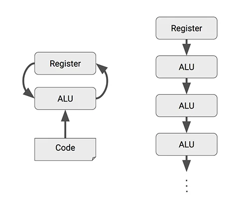
The process of performing arithmetic operations such as addition or multiplication in a general processor is as follows:
- Load data into register
- Controller sends commands to ALU (Arithmetic Logic Unit)
- ALU reads data from register, performs operation, and writes result back to register
In other words, every time an ALU performs an individual operation, it needs to read data from and write to registers. Large-scale matrix operations used in AI require significantly more computation than general operations. If we could eliminate this process:
- We could increase area efficiency by reducing required register capacity
- We could reduce power consumption by decreasing data movement between register ↔ ALU
Systolic array is one alternative that can eliminate this process. Instead of storing the results computed by individual ALUs in registers, it passes them to other ALUs. This achieves the effects mentioned above.
However, to effectively use Systolic array, several conditions must be met:
- The timing for passing data between ALU → ALU must be precisely synchronized
- It must be guaranteed that results computed by individual ALUs are used in the next ALU
While the first condition can be controlled appropriately at the hardware level, the second condition must be satisfied by the nature of the operation itself. Interestingly, matrix multiplication satisfies this condition, making Systolic array the most efficient for this purpose.
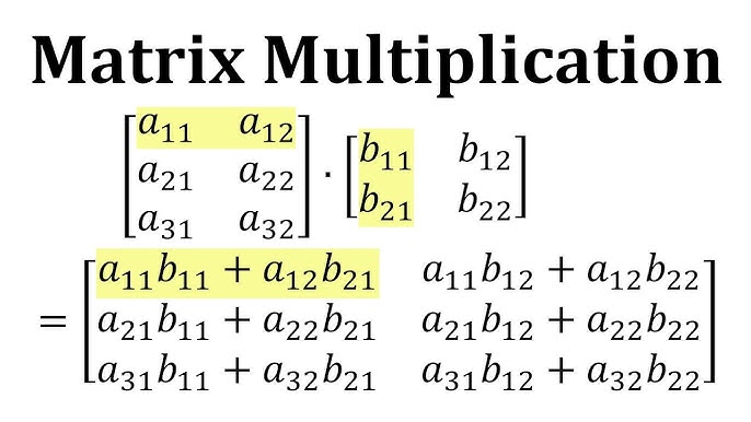
Matrix multiplication can be decomposed into multiple vector dot products. A vector dot product is the accumulated sum of individual element multiplications. By precisely synchronizing the timing of elements entering individual ALUs as input and passing the multiplication values to the next ALU while sequentially accumulating, matrix multiplication can be performed without communication with registers.
This Systolic array is a representative feature used in TPU and has had a significant impact on GPUs and other AI accelerators (NPU, LPU) that perform AI operations.
TPU Building Block
Next, let’s examine the computation units used in individual TPU chips. As we saw earlier, GPUs consist of hundreds of SMs (Streaming Multiprocessors). The hardware scheduler selects warps (32-thread bundles) that are ready for execution in real-time and feeds them into computational resources. This is not about executing instructions randomly, but rather a method of maximizing efficiency by filling waiting time with other tasks (Latency Hiding). In other words, GPUs are optimized for maximizing overall throughput by densely managing numerous small computational units.
In contrast, TPU (Tensor Processing Unit) takes a contrasting approach. Instead of numerous finely divided units, TPU is equipped with a small number of powerful dedicated cores capable of processing massive matrix operations at once. It also operates by pushing large amounts of data into computational blocks at once through higher-level instructions (VLIW, Very Long Instruction Word) that combine multiple instructions. Rather than relying on complex dynamic scheduling, TPU architecture is designed to perform large-scale matrix multiplication—the core of AI operations—in a single pass, like a massive pipeline flowing through, which is the essence of TPU architecture.
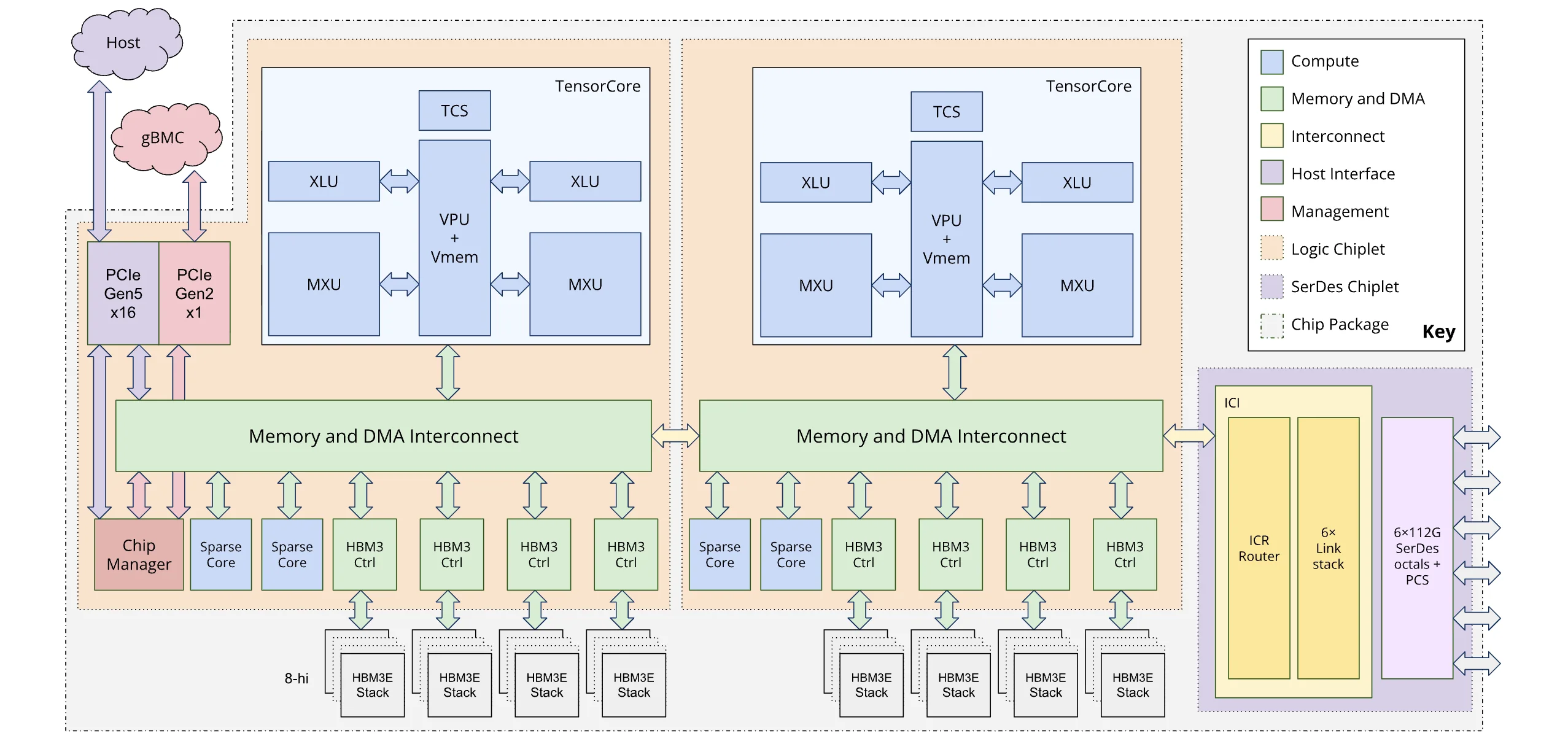
The cores used in individual TPU chips are divided into TensorCore, specialized for linear algebra operations, and SparseCore, specialized for embedding operations. (Note: While the terminology is the same as GPU’s Tensor Core, their roles differ.)
TensorCore
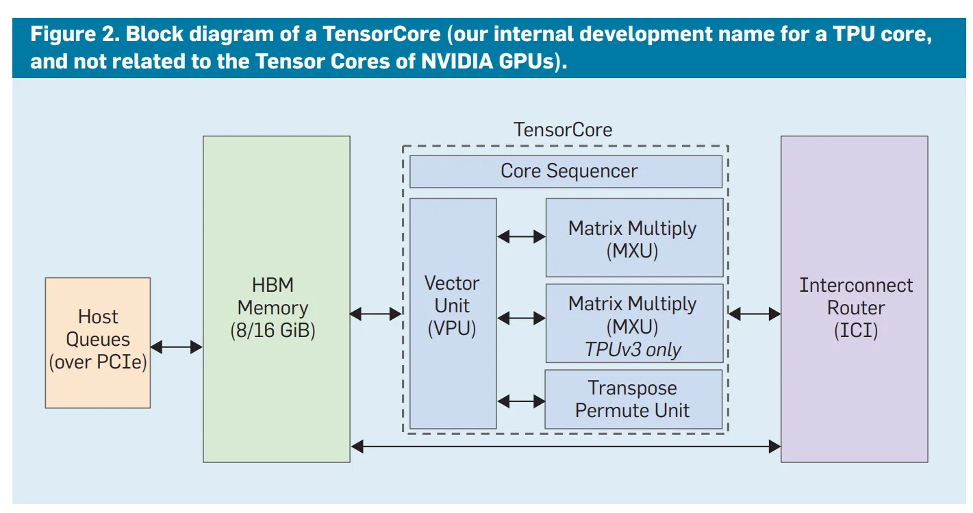
TensorCore is a computation pipeline that performs operations on data delivered through Systolic array and DMA (direct memory access) units. Similar to GPU’s CUDA cores or Tensor cores, while GPUs cannot specify exactly which core to use at which time (automatically filling available execution units), TPU’s TensorCore is statically allocated according to dataflow optimized at compile time. The MXU (Matrix Multiplication Unit) for matrix operations mentioned earlier is the most representative, and it also includes operators for scalar and vector operations, not just matrix operations. Depending on the generation, 1 or 2 TensorCores are mounted per chip.
SparseCore
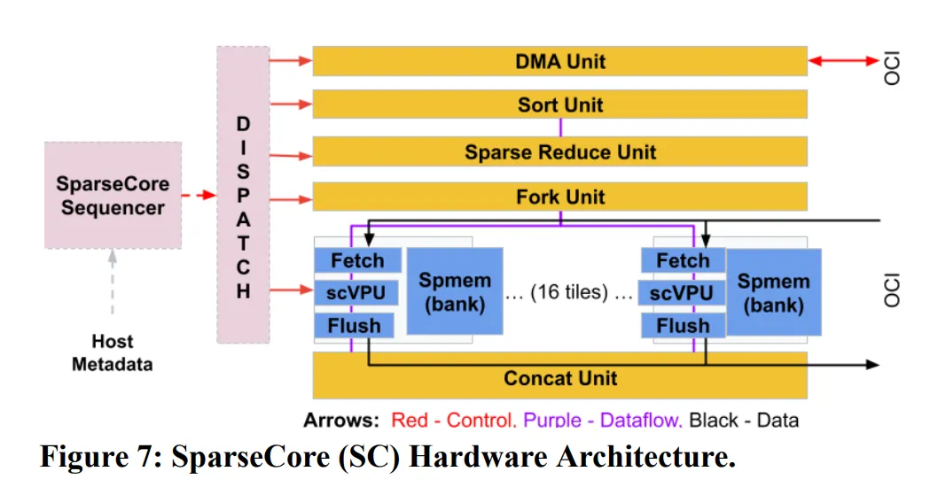
SparseCore is a core architecture applied from the 4th generation TPU. SparseCore is a unit specialized for embedding operations, one of the operations used in AI besides matrix operations. While embedding operations used in LLMs have relatively small table sizes and don’t have excessive computational overhead, in recommendation systems like DLRM (Deep Learning Recommendation Model), embedding table sizes can account for most of the total parameters, making the overhead very large, so there’s a very high probability of computational bottlenecks in embedding operations.
The proportion of SparseCore in TPU (based on 4th generation) is about 5%, small compared to TensorCore, but this unit achieved 5-7x performance improvement compared to before. Depending on the generation, 2 or 4 SparseCores are mounted per chip.
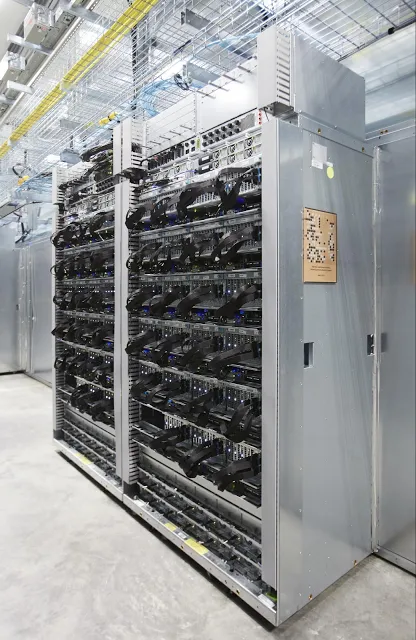
Scale-up/Scale-out System
TPU performs operations with a small number of massive cores, 1-2 per chip. While it’s possible to perform operations with a single chip using massive cores, connecting multiple chips and using them in parallel is necessary for larger operations. TPU uses the following network technologies for this purpose.
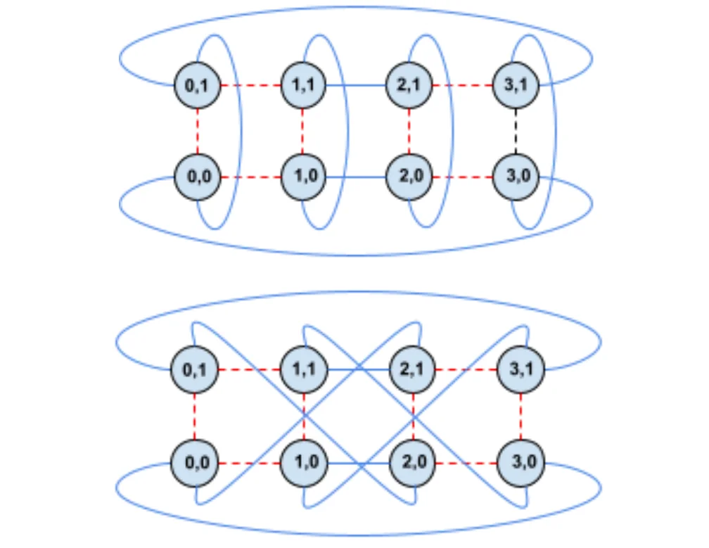
Torus Topology
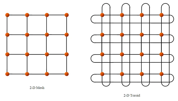
TPU uses torus topology for scale-up, connecting multiple chips to build one massive server. When thinking about connecting multiple chips, one typically imagines a grid structure like a Go board (mesh topology) as shown in the first figure. The disadvantage of this structure is that nodes at both ends are not connected, making the maximum distance between nodes longer. In the torus structure, nodes at both ends are connected with wrap-around links, increasing wiring complexity but reducing the maximum distance between nodes from N to N/2. In the 4th generation TPU, this torus structure was extended to 3D, expanding the communication range between nodes and the number of TPUs grouped together. A group of 4 * 4 * 4 (=64) TPUs is called a cube, and a cluster of multiple cubes is called a pod.
Optical Circuit Switch (OCS)
A network switch is needed to mediate communication between chips. TPU introduced OCS, an optical switch, to allow the connection structure between torus networks to be reconfigured in software. This enables software to determine the optimal connection structure according to computation characteristics.
TPU Software Stack
Next, let’s examine the software used in TPU.
TensorFlow
As mentioned in the previous post, GPUs can be controlled through CUDA, a programming model. Instead of developing a kernel language like CUDA, Google developed a deep learning framework called TensorFlow that can be used regardless of GPU or TPU.
The characteristic of frameworks like TensorFlow and PyTorch is that, unlike CUDA, developers can execute the same code on various accelerators like GPU and TPU immediately without understanding the detailed structure of the hardware. Google provided strong flexibility so that the same TensorFlow source code could run on various hardware platforms (CPU, GPU, TPU) and be deployed anywhere from mobile devices to large-scale distributed systems for ecosystem expansion. This made TensorFlow a powerful tool for industry/deployment. However, precise hardware control is difficult, so there are limitations from an optimization perspective.
JAX
However, there is a way to optimize TPU hardware at the software level. This is possible using JAX, a Python library. This is a Python library developed by Google internal developers who actively use TPU to use TPU more efficiently. TPU can use XLA, a machine learning acceleration compiler that will be explained shortly. XLA is a compiler that can be used in both TensorFlow and JAX. JAX is a kind of Python interface created for software developers to use this XLA more directly and flexibly. It can be used regardless of GPU/TPU, and provides functional programming paradigms and automatic differentiation capabilities, making it more suitable for research and experimentation. Google’s AI team actively uses it for research and model training, but it has a somewhat high barrier to entry because operations must be optimized at the software level.
XLA (Accelerated Linear Algebra)
Google began to consider ways to overcome the limitations of TensorFlow mentioned earlier and further improve TensorFlow’s performance in machine learning. Google likely had two main directions to choose from:
- Create a separate low-level language (e.g., TPU-C) that can directly control hardware similar to CUDA, and create optimized kernels that can be called from high-level languages like TensorFlow
- Use a compiler specialized for machine learning to generate machine code optimized for that hardware
The former approach gives developers direct hardware control, providing high freedom. Additionally, whenever new features are added to hardware or new algorithms (FlashAttention, Mixture-of-Expert (MoE)) are developed, developers must write new CUDA kernels for optimization. The demand for optimization always exists, and each time, the CUDA ecosystem expands. This acts as a huge technical moat in the CUDA ecosystem that makes it difficult for other hardware companies to enter the market.
Google chose the latter approach, creating the XLA compiler specialized for linear algebra operations, which are central to machine learning operations. While they avoided directly challenging the CUDA ecosystem, you could say they shifted the burden of developers having to learn new languages to the compiler. Let’s examine how the XLA compiler optimizes operations through some AI operations.
(* This explanation is an example to illustrate the optimal approach of the XLA compiler and does not match actual operation.)
import math

# 1. Linear: z = weight * x + bias
def linear_op(x, weights, bias):
    # write result to main memory
    z = [sum(xj * wj for xj, wj in zip(x, weights[i])) + bias[i]
         for i in range(len(weights))]
    return z

# 2. Activation: ReLU
def relu_op(z):
    # Read z value from main memory -> write back result to main memory
    a = [max(0, val) for val in z]
    return a

# 3. Softmax
def softmax_op(a):
    # read a from main memory -> find max -> summation -> div -> write back result to main memory
    max_val = max(a)
    exp_vals = [math.exp(val - max_val) for val in a]
    sum_exp = sum(exp_vals)
    return [ev / sum_exp for ev in exp_vals]
Simply executing the above 3 functions sequentially requires writing intermediate results of each function to main memory and reading them again. The core of the XLA compiler is to integrate these operations, remove unnecessary computations or memory allocations, and perform operations with fast speed and low memory usage.
GPUs can also integrate multiple operation kernels through kernel fusion. While GPUs have two methods - manually creating integrated CUDA kernels and automatically fusing kernels using PyTorch or TensorRT internal features - XLA differs in that it analyzes individual operations at compile time and generates machine code optimized for each hardware (CPU/GPU/TPU).
XLA was supported in TensorFlow and JAX, and recently its base has expanded as PyTorch also supports XLA through pytorch/xla.
Pallas
XLA is a powerful optimization compiler, but it has limitations. When new operation algorithms emerge, it’s difficult for manually created custom kernels to match performance until the compiler is updated to a version that can optimize them.
To address this, Google has been providing a kernel language API called Pallas (jax.experimental.pallas) as an experimental extension of JAX since around 2023. This corresponds to the first of the two methods mentioned earlier for performance improvement. Pallas can be compared to Triton, a high-level kernel language for GPUs born in 2021.
Triton is an open-source GPU programming language created by OpenAI in 2021. It overcomes CUDA’s limitations of high barriers to entry and requiring understanding of hardware structure by providing a more abstracted interface than CUDA, enabling machine learning developers to more easily optimize various operations and algorithms on GPUs. It abstracts away from Hopper/Blackwell and other architectures to increase developer convenience, and despite the high level of abstraction, there are benchmarks showing that programs created with Triton reach similar performance levels to manually created CUDA kernels.
Integration to use Triton language in JAX has also progressed, but since Triton only works on GPUs, it was difficult to perform such optimizations on TPU. Pallas is a TPU kernel-language API created to overcome this, and unlike Triton, it provides a common kernel language that supports both GPU and TPU, which is its major feature. Pallas has been integrated not only in JAX but also in PyTorch/XLA.
Ironwood Launch: Google’s Declaration of Entry
After the 4th generation TPU, there isn’t much detailed technical documentation, so we’ll discuss what changed in the 7th generation TPU compared to previous generations and what it implies for the AI semiconductor industry from a technical perspective.
Hardware Perspective
Chiplet Architecture
Ironwood is the first TPU architecture to adopt chiplet structure. Chiplet structure is a process technology introduced to overcome the limitations of semiconductor manufacturing processes called the reticle limit.
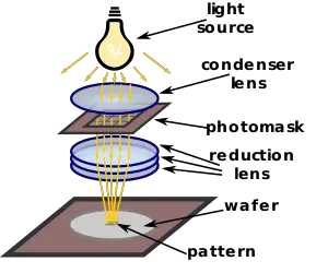
Reticle Limit: The reticle limit refers to the maximum size of an individual die that can be produced in a single exposure, determined by the reduction ratio of the lens in the lithography equipment used to draw circuits on the photomask (reticle), which is standardized and fixed in the semiconductor industry. When this limit (currently approximately 858mm²) is exceeded, single exposure becomes impossible, requiring a stitching technique that connects multiple exposure patterns. However, in this case, defect rates increase rapidly and manufacturing costs rise. For these economic reasons, existing chips were manufactured so that the processor area (area other than memory) did not exceed this size.
However, as the demand specifications for chips used in data centers increased, larger chips became necessary, and instead of increasing single chip size, chiplet structure was introduced, where chips are split into multiple chips of the same structure and connected at the packaging stage. This allows individual chip sizes to increase, enabling individual product performance to increase.
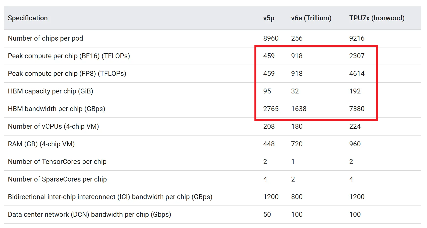
NVIDIA GPUs introduced this technology starting with the Blackwell architecture B100/B200 product line released in 2024, and other accelerator companies making data center accelerators are also adopting this structure. TPU applied chiplet structure starting with this generation’s product line, and we can see that single product performance (peak compute, memory bandwidth, etc.) is significantly higher than previous generations.
In this chiplet structure, since 2 individual dies show performance beyond individual chips of previous products, Ironwood treats individual dies as one node in torus topology, enabling individual control. For this, 4D torus topology was introduced by adding one more axis to 3D torus.
Software Perspective
vLLM Support and the Emergence of tpu-inference
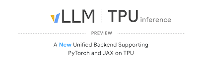
Google integrated a new hardware plugin called tpu-inference into vLLM last October. This plugin unifies JAX and PyTorch into a single lowering path, generating optimized TPU machine code regardless of framework. The biggest advantage of this plugin is that it enables high-performance LLM model serving on TPU using the same vLLM interface used on GPU.
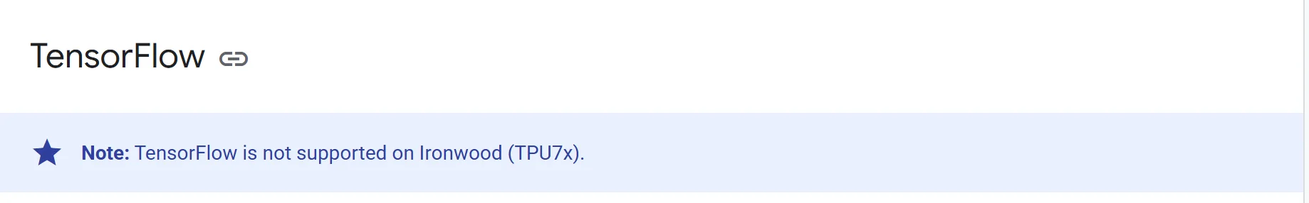
TensorFlow Support Discontinuation
Google boldly discontinued TensorFlow support starting with this generation TPU. This is interpreted as having two meanings: acknowledging PyTorch’s ecosystem dominance while integrating XLA into the existing ecosystem to optimize TPU performance within the PyTorch ecosystem (PyTorch/XLA), and focusing more on the JAX framework, which is more optimized for performance improvement than TensorFlow for independent framework development.
Pallas’s Establishment in the Software Ecosystem
Although Pallas is still documented as an experimental feature in JAX official documentation, Google officially introduces Pallas as a means to maximize TPU performance in their blog. This is interpreted as encouraging developers to write optimized kernels directly without waiting for XLA compiler updates. The freedom of kernel optimization that existed in CUDA/Triton can now be enjoyed on TPU as well.
Google’s Ambition in the AI Semiconductor Market
This expansion of the software ecosystem and dramatic improvement in hardware performance means more than just technical improvement - it represents Google’s strategic shift. This is a move to formally enter the AI semiconductor market that NVIDIA has monopolized. Let’s examine Google’s market entry strategy below.
Direct TPU Sales Possibility
Until now, TPU could only be leased through Google Cloud (GCP). For security reasons, detailed hardware technical documentation was not publicly disclosed, and direct sales were not conducted, so TPU existed only in Google’s internal data centers. However, it’s been reported that Google is considering strategies to directly supply TPU to third-party data centers or sell the hardware itself. This is a declaration to shed the image of a closed Google-exclusive chip and compete head-on with NVIDIA as an independent AI semiconductor vendor.
Software Openness and Completion of Vertical Integration
NVIDIA’s strength comes not only from hardware but also from the CUDA software ecosystem. Google is countering this with XLA automation and Pallas openness as weapons. They’re sending the message: “GPUs require manual kernel optimization for best performance, but TPU automatically optimizes through the compiler and developers can also tune directly if needed.” Moreover, Google’s software stack, unlike CUDA, is not limited to specific hardware, enabling competitive advantage in the emerging heterogeneous computing market.
Furthermore, Google is the only company that has vertically integrated the entire AI stack: models (Gemini), frameworks (JAX), compilers (XLA), and hardware (TPU). In the AI semiconductor market where software and hardware integration is essential, Google has secured an advantageous position through this vertical integration.
Summary
In this article, we explored:
- The background of TPU’s emergence
- TPU’s hardware/software architecture
- Features of the latest TPU product, Ironwood
- Google’s semiconductor market strategy
The conclusions we can draw from this are summarized below:
- Google has been developing TPU, an ASIC optimized for AI workloads, for 10 years.
- They continue their technical efforts to break down the technical moat of GPU and CUDA and build a software ecosystem that is not hardware-dependent.
- Beyond simple cloud business, they aim to directly enter the AI semiconductor market and establish equal status with NVIDIA.
Did you know that members who participated in the original TPU project had founded another semiconductor startup? Groq, an AI semiconductor startup that recently signed a contract worth approximately $20 billion (30 trillion KRW) with NVIDIA, is that company. What technology did NVIDIA pay such an enormous amount for? In the next article, we’ll explore Groq’s LPU, which uses the same terminology as us.
Reference
- An in-depth look at Google’s first Tensor Processing Unit (TPU)
- From silicon to softmax: Inside the Ironwood AI stack
- Announcing Ironwood TPUs General Availability and new Axion VMs to power the age of inference
- In-Datacenter Performance Analysis of a Tensor Processing Unit
- TPU v4: An Optically Reconfigurable Supercomputer for Machine Learning with Hardware Support for Embeddings
P.S.: HyperAccel is Hiring!
Knowing your enemy and yourself is important, but to truly win we also need great people on the team.
If you’re interested in the kinds of technologies we work on, please apply via HyperAccel Career.
We’re looking forward to hearing from talented engineers like you.